


MPW service for MEMS gas sensor
We start MPW (Multi Project wafer) service for the MEMS gas sensors.
Many customers are facing a significant burden in the initial development costs for MEMS devices. You can develop the product you want at a predetermined cost to relieve the burden.
This is a method to proceed with the process by inserting a number of companies designs in a mask. If eight companies participate into eight regions on a single mask, it can be produced from one wafer products for the respective companies at the same time.
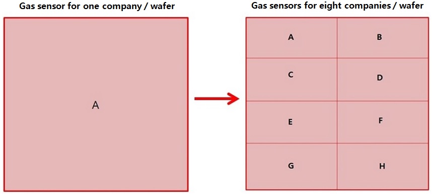
After finishing the fabrication, each compay will receive a delivery of each product. Of course, it will fit with NDA agreement to proceed.
The following are, in reference to customer to design the MEMS gas sensors.
1.A description of the basic structure of a MEMS gas sensor.
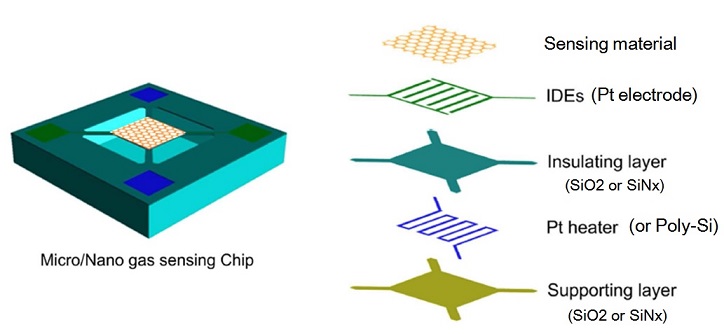
The abow picture shows the overall structure of the membrane sustained by four anchors. There is a layer of air under the membrane structure that is easy to keep up the temperature increased by a heater. At a constant temperature to some extent, sensor reacts with specific gas. The membrane is basically made up of five layer thin film, the material on each film is as in the picture above.
2. A description of the simulation for MEMS gas sensors.
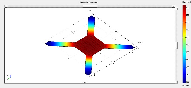
The above figure shows that the temperature is kept when the electric power is applied to the wire in a square membrane, the size of 200um × 200um and the phenomenon that heat escape through the anchor with modeling.
This is the result of a simulation by setting a length, width and thickness parameters of the Pt thin heating wire. This is an exampleof more than 500 degrees C temperature implemented in a power of about 15mW or so. ( shown in Figure absolute temperature.)
Most of the gas sensing materials react with gas at a temperature of that degrees.
Customers can proceed with the mask design after simulating cantilever bending, yield strength, and the reliability test, etc. You can ask for simulation or mask design to us.
3. A brief description of the layout.
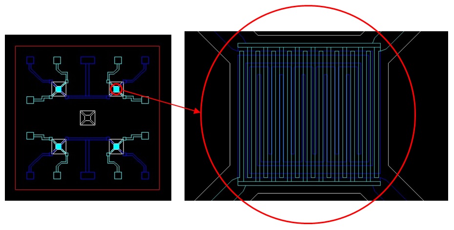
The figure above is an example of a mask layout design, 2 × 2 array-type MEMS gas sensors. In consideration of the process order, the mask is designed to start a thin-film gas sensor MEMS processing.
Refering to the above, after customers proceed to the simulation and layout design for the MEMS gas sensors, please send us the file along with the down payment. .If some companies have gathered to participate in the MPW service, wafer level gas sensor chips will be fabricated.
Most of the production process from the mask is produced in the foundry line in Korea. The final process of gas sensing material is to be doped by customers to develop after delivered.
Please apply MPW service :
e-mail : nano@nano-i.com
Phone : 82-70-8827-9577 , Cell phone 82-10-4293-9577
R&D
The following informations are about our technology deveopment such as MEMS design, nano-MEMS applications (3D laser scanners, 3D laser display, underwater ultrasonic sensors and circuits, etc.), video intelligence, and developing applied technology and other service-related knowledge as possible available information. It will be continuously updated.
-
read more
드론 기반 리튬 광산 염수 수위 측정 장치
본 제품은 드론 기반 리튬광산 염수 수위 측정 장치입니다. 본 제품은 리튬 광산의 염호(염수 호수) 내 염수 수위를 정확하게 측정하여, 리튬 농축 효율 관리 및 채굴 최적화를 실현하기 위한 드론 기반 리튬광산 염수 수위 측정 장치입니다. 드론 기반...Date2025.04.21 -
read more
자이로 센서 및 오도미터 응용 지하 매설관 내 GPS 좌표 측정 장치
본 제품은 자이로 센서 및 오도미터를 응용하여 지하 매설관 내 GPS 좌표를 측정하는 장치입니다. 본 제품은 자이로 센서 및 오도미터를 응용하여 지하 매설관 내 GPS 좌표를 측정하는 장치입니다. ( 고객 : 강산 기술) 매설관 입구에서 GPS 좌표를 측정...Date2022.09.29 -
read more
고분해능 니켈 금형 및 마이크로 렌즈 어레이
고분해능 니켈 금형 및 마이크로 렌즈 어레이 고분해능 니켈 금형 및 마이크로 렌즈 어레이제작에 대한 내용입니다. 본 제품은 HD 급 이미지 센서 또는 고밀도 라이다 용으로 사용되어지는 마이크로 렌즈 어레이 용 니켈 금형 및 마이크로렌즈 ...Date2022.09.28 -
read more
싱크홀 크기 측정용 3D 레이저 스캐닝 라이다
본 제품은 싱크홀 크기 측정용 3D 레이저 스캐닝 라이다입니다. 최근 도로 등의 지하 공간에서는 싱크 홀 등의 문제로 보수 공사하는 경우가 많이 발생하고 있습니다. 보수 공사하기 위하여서는 시추홀의 크기가 외경 50 mm 이내로 한정되어 있어서 그 비...Date2022.02.09 -
read more
대면적 마이크로 렌즈 어레이용 금형 개발
대면적 마이크로 렌즈 어레이용 금형 개발에 대한 내용입니다. 일반적으로 마이크로렌즈어레이의 단위 렌즈 크기는 수마이크로미터 내지 수백마이크로미터 크기의 직경을 가지나, 당사가 개발한 대면적 마이크로렌즈 어레이용 금형은 렌즈의 크기가 수 mm 정도...Date2022.02.05 -
read more
반구형 마이크로 렌즈 어레이 개발
반구형 마이크로 렌즈 어레이 개발 반구형 마이크로 렌즈 어레이 개발에 대한 내용입니다. 당사가 공개했던 마이크로 렌즈 어레이 (https://www.nano-i.com/webjin_development/1274460) 에 대한 응용 기술 개발에 대한 내용입니다. ...Date2021.03.07 -
read more
MEMS 가속도 센서 개발
MEMS 가속도 센서 개발 정전 구동 MEMS 가속도 센서 ( MEMS Electrostatic actuating acceleration sensor ) 설계에 대한 내용입니다.. 멤스 초창기부터 가속도 센서 개발에 뛰어든 선두 주자들이 현재 전 세계 MEMS 시장을 주도하고 있습니다....Date2021.03.06 -
read more
자이로 GPS 로라 통합 모듈
자이로 GPS 모듈 본 제품은 2018년 4월에 개발하였던 GPS 로라 블루투스 융합의 자이로센서 모듈입니다. 물체의 위치 (GPS 좌표)와 회전각도를 멀리서도 정확히 실시간으로 알 수 있습니다. 제품 또는 응용 기술 개발 문의 연락처 : 010-4293-9577, e-...Date2018.12.31 -
Read More
MPW service for MEMS gas sensor
MPW service for MEMS gas sensor We start MPW (Multi Project wafer) service for the MEMS gas sensors. Many customers are facing a significant burden in the initial development costs for MEMS devices. You can develop the product you wa...Date2016.05.23 -
Read More
농약살포용 자율주행 로봇 개발 (라이다/자이로 센서 응용)
농약 살포용 자율 주행 로봇 개발 본 제품은 당사가 개발한 농약 살포용 자율주행 로봇으로써, 비닐하우스 등 농약 살포를 하면서 장애물을 회피함과 동시에 정해진 경로로 자율 주행을 할 수 있는 로봇입니다. 레이저를 사용하여 주변의 16m 이내의 거리를 36...Date2017.12.11 -
Read More
열교환기용 마이크로 채널 개발 (고객 : 동경대학교)
본 제품은 일본 동경대학교의 주문으로 개발한 제품이 되겠습니다. 1. 마이크로 채널 (가공기술 : MEMS) 재질 : 스테인레스 (SUS, 1.5 t) 마이크로 채널 : - 채널 수 : 4 채널 - 750 um x 500 um x 118 mm , 17 개 @ 1 채널 ...Date2015.04.08 -
Read More
고속 3차원 레이저 스캐너 개발
제목 : 마이크로 전기 기계 시스템 응용 고속 3차원 측정용 라이트 엔진 개발 사업명 : 중소기업진흥공단 지원 아이디어 상업화 지원 사업 개발 기간 : 2009.08.01 ~ 2010.05.30 특허명 : 3차원 스캐너용 측정 장치, 특허 등록 번호 : 1011624390000 ...Date2013.10.04 -
Read More
3차원 레이저 디스플레이 개발 (세계 최고급 색재현율)
제목 : TV 급 3차원 레이저 캐릭터 영상 시스템 개발 사업명 : 중소기업기술정보진흥원 지원, 팀 기술개발 지원 사업 개발 기간 : 2011.09.01. ~ 2012.06.30. 양안 시차 적용의 두 개의 프로젝터로 구현되는 848 x 480 어레이의 분해능, 밝기 24 lumen의 R,G,...Date2013.10.06 -
Read More
(40가지 해결 원리 적용) MEMS 구동 거울 개발
1. 종래의 MEMS 구동 거울 Nippon signal Fraunhofer Institute Mirrorcle Tech. 2. 기술적 모순 : 레이저가 거울 표면에서 반사되기 위하여 경사 각도로 입사 시, 거울 ...Date2013.10.03 -
Read More
수중 초음파 센서 및 회로
수중 초음파 센서 및 회로 : 응용 분야 - 강, 호수 등의 깊이 측정 공동 개발 : 중앙대학교 1) 수중 초음파 센서 2) 초음파 발진 및 수신 회로 개발 (Firmware 포함)Date2013.10.04 -
Read More
(실험 계획법 적용) 적외선 센서를 응용한 터치 스위치 또는 패널 개발을 위한 최적 조...
본 건은 장갑을 끼고도 터치할 수 있는 스위치 센서를 개발하기 위한 인터페이스를 개발하는데 있어서 햇빛 조명 등 외부 환경 요인에 대하여 가장 최적의 터치 조건을 실험 계획법으로 나노아이사가 고객의 요청으로 개발한 사례이다. 본 건은 장갑을 끼...Date2014.03.02 -
Read More
(이상해결책) 적외선 센서를 응용한 터치 스위치 또는 패널 개발
본 건은 실험계획법으로 개발한 조건에 대하여 현재의 문제점을 분석하고, 이상해결책을 창의적으로 도출하는 방법을 간단하게 제시한 예입니다. 자세한 절차나 방법에 대한 문의는 아래 연락처로 연락 부탁드립니다. e-mail : nano@nano-i.com 연락처 : 010...Date2014.03.09 -
Read More
고출력용 마이크로 렌즈 어레이 (설계 단계의 성능 검증)
고출력용 마이크로 렌즈 어레이 (Micro lens array for high power) 고출력용 마이크로 렌즈 어레이 개발 일반 마이크로 렌즈 어레이 (Micro lens array) 는 보통 폴리머를 사용하였으나, 당사는 고출력용으로는 쿼츠 재질의 마이크로 렌즈 어레이...Date2014.04.28
Designed by sketchbooks.co.kr / sketchbook5 board skin
Sketchbook5, 스케치북5
Sketchbook5, 스케치북5
Sketchbook5, 스케치북5
Sketchbook5, 스케치북5

